
| Home | S-100 Boards | History | New Boards | Software | Boards For Sale |
| Forum | Other Web Sites | News | Index |
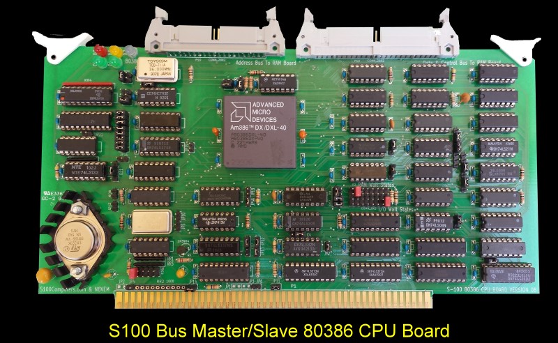 |
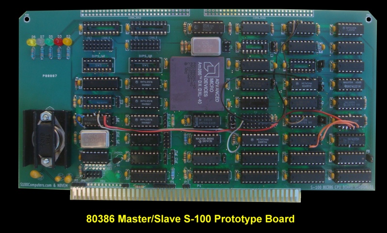
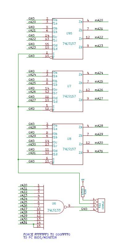
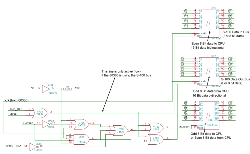
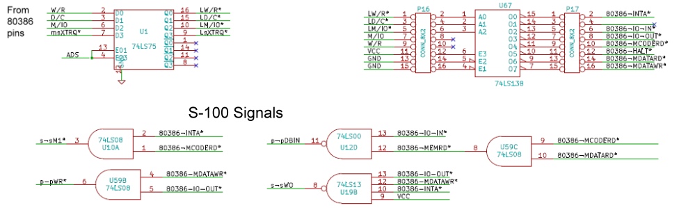
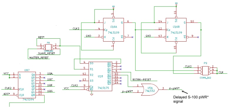
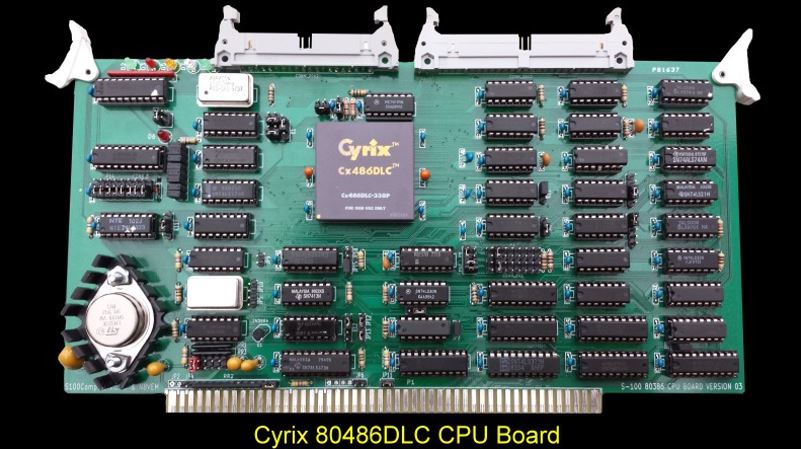
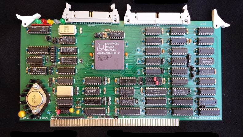
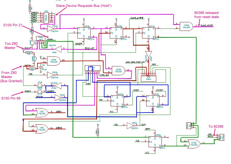
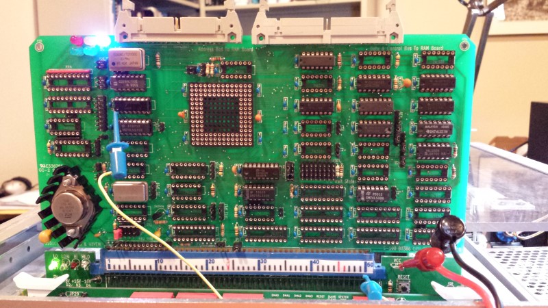
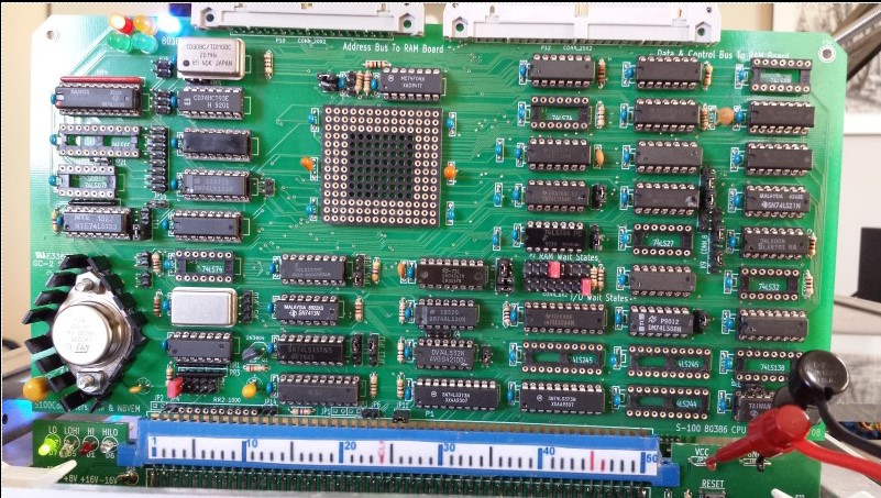
| 1 | Build and debug Master/Slave S-100 80386 CPU board such that it is completely self-contained and can run MS-DOS in the system on the S-100 bus. | |
| 2 | Build a ribbon cable connected S100 daughter RAM board utilizing very high capacity static RAM chips (16M chips). | |
| 3 | Build the same type of board utilizing very high capacity DRAM SIMMS (1GB SIMMS). |
 |
 |
 |
 |
 |
 |
|
 |
 |
 |
 |
 |
 |
 |
 |
 |
 |
 |
|
|
 |
|
 |
This page was last modified on 10/08/2022